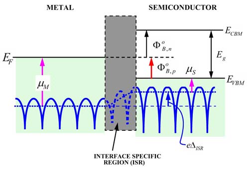
The distributions of crystal potential, -eV(r), (solid blue lines)
and energy bands (solid straight black lines) at a metal-semiconductor
interface. The average crystal potential is drawn as dotted blue line.
Band bending has been ignored in this diagram.

FoB,p =
mM -
mS -
eDISR